
The new technique increases the luminescent efficiency of semiconductor particles by about 9,000 times by using multifunctional tip-enhanced spectroscopy and dynamic control.
It has been demonstrated that semiconductor particles can be controlled using multifunctional tip-enhanced spectroscopy to increase their luminance.
Researchers from ITMO University in St. Petersburg, Russia and the Pohang University of Science and Technology (POSTECH) in South Korea worked together to create a novel technique for controlling the physical characteristics of semiconductor particles in real-time (1).
The new technique increases the luminescent efficiency of semiconductor particles by about 9,000 times by using multifunctional tip-enhanced spectroscopy and dynamic control.
In materials science, a method called multifunctional tip-enhanced spectroscopy is used to examine the nanoscale characteristics of materials. It involves producing a strong electric field with a sharp probe tip to increase the sensitivity of different spectroscopic measurements.
The method can be used to investigate a material’s surface structure, chemical make-up, and optical and electronic characteristics.
The method holds promise for creating new kinds of semiconductor devices and optoelectronic materials by giving a way to dynamically control the physical characteristics of quasiparticles, such as interlayer excitons and trions.
Interlayer excitons, electrically neutral quasiparticles that can be used in next-generation semiconductor devices because of their mixture of light and matter, were the main focus of the team’s research. The interlayer excitons’ luminous energy can also be modulated by the new method, giving researchers control over the colour of the light.
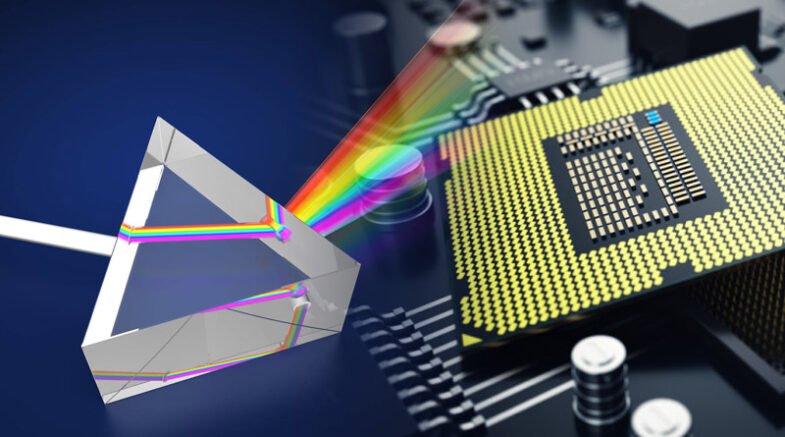
Micron-sized particles known as semiconductors are composed of substances with electrical conductivities that fall between those of insulators and conductors. These particles are used in a variety of electronic components, including light-emitting diodes, transistors, and solar cells (LEDs).
By using hot probe tip technology to raise the spatial resolution to 20 nm, the team created the new technology. Through this method, they were able to dynamically control the physical characteristics of quasiparticles at room temperature and normal atmospheric pressure.
This innovation will be crucial in creating wearable optoelectronic devices with high luminance and extreme thinness. The new approach developed by the research team is anticipated to expand the range of applications for two-dimensional (2D) semiconductors based on heterostructures.
The team hopes that the new technology will be used to identify new physical properties of individual semiconductor particles, which could lead to the discovery of new materials that go far beyond the performance of existing materials.
The accomplishment is especially noteworthy in the current environment, where nations like China, Japan, and the United States compete for dominance in the semiconductor equipment market and erect technological barriers. The researchers’ innovation in the design of measuring instruments significantly influenced the outcome and attracted additional interest in the field.
The development of wearable electronics that are both soft and thin and have a wide range of electrical and optical capabilities is made possible in large part by this innovation.
The development of next-generation materials for the electronics industry depends on being able to create new materials that perform significantly better than those currently available. The new method created by the POSTECH team may make it possible to produce Spiderman-like suits that are soft and thin but have numerous functionalities.
In conclusion, the development of next-generation semiconductor devices is anticipated to be significantly impacted by the discovery made by the POSTECH team. A new generation of wearable optoelectronic devices may be developed using the team’s novel technique for real-time control of semiconductor particle physical properties.