
Through research, the development of Advanced Material like carbon nanotubes (CNTs) and other two-dimensional materials such as graphene
Through research on Advanced Material, the development of Materials like carbon nanotubes (CNTs). Other two-dimensional materials (such as graphene and GO) have depicted marvellous suitability in detecting various chemical and biological molecules. Moreover, as well other analysing variables e.g. temperature, pressure and humidity. The dominant basic electronic properties of such materials permits for the designing of more sensitive and selective devices. While on other hand also lowering the cost, small size and power consumption of those sensors for temperature and pressure measurement.
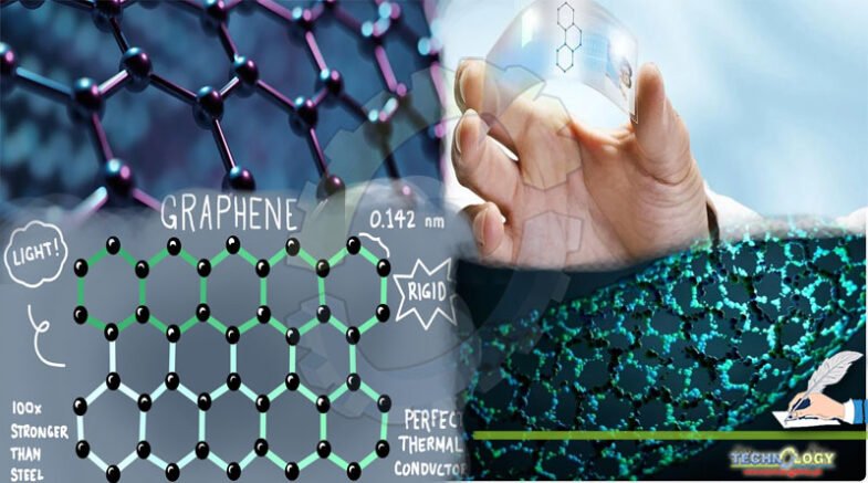
Graphene:
Graphene, an Advanced Material, and its derivative materials have now introduced new significant applications. This is because of their unique structure and low toxicity, as well as excellent electronic, electrochemical, and mechanical properties. It has a two-dimensional (2-D) sheet of carbon atoms in a hexagonal form (honey-comb structure) with unique properties. Furthermore, such as a large surface area (~2630 m² g−¹), high Young’s modulus (~1 TPa), marvellous thermal conductivity (~5000 W m−¹ K−¹), good charge carrier mobility (2 × 105 cm² V−¹s−¹) due to π-conjugation structure; involves clear optical transparency (~97.7%).
These are some of the reasons that Advanced Material graphene-based nanocomposites have edge roles in different devices and applications. It can also be easily used in gas sensing applications with other Advanced Materials as composites (Metal-Organic Framework, Polymeric, and heterostructures, etc.)
Suitability of Graphene:
One of the most important characteristics of Advanced Material graphene is that give it an edge over other candidates in gas sensing applications. The Advanced Material have Specific Surface Area (SSA), Change of interaction between graphene sheets and adsorbents molecules, High mobility electron-hole pair at room temperature, Low Electrical noise factor, Large scale Fabrication Capacity.
Graphene Structure & Application:
In Advanced Material such as graphene single-layered sheets, almost all the atoms are surface atoms. In this form, all atoms can be adsorbing gas molecules since graphene and its derivative ; can be providing the largest sensing area per unit volume. This thing also enhances graphene and absorbent molecules’ interaction chances. Due to which, easy adsorption and as well as low sensing easily occurred.
The intermolecular attraction between graphene sheets and adsorbates gases could occur via different forces, such as a weak van der Waals interaction and a relatively strong covalent bonding. The electronic structure of graphene could be perturbed by such different molecular forces, and this change in the electronic movement can be readily monitored by convenient electronic techniques.
The electronic structure of graphene Advanced Material also depicts very high carrier mobility at just room temperature (2 × 105 cm² V−¹ s−¹) with an electronic charge density of near 1012 cm−², since it is as more conductive as that of silver, and it has the relatively lowest resistivity at room temperature resulted in resistivity of 10−6. This is well known that carrier mobility plays a vital role in gas sensing devices. For that purpose, Advanced Material graphene has been introducing as a highly sensitive gas sensor because of its extraordinary charge carrier mobility, which has made it a unique and attractive sensing material for gas sensing applications.
It has a very high-quality crystal lattice along with its 2-D structure that results in low electrical noise phenomena. Since this structure making it capable of damping more charge fluctuation, which a few numbers of extra electrons, and gas adsorption even on a molecular level, can make a noticeable change in the conductance or resistance of a graphene film.
Future Developments:
Metal oxide semiconductors (MOS) are the effective materials for gas sensors from some last few years. Moreover, for commercial fulfilment as of the 4-S criterion isn’t fulfilling. From the fundamentals of the Advanced Material MOS sensing mechanism, most surface morphologies and hetero-structure interfaces are involved. In short, these classifications of sensors typically have an awfully high operating temperature (>400°Celsius). One of few biggest drawbacks for such sort of gas sensors, and it restricts their practice due to ; sometimes very low selectivity and particularly less stability. After the invention of Advanced Material, like carbon nanotubes in 1991, graphene in 2004; their functional and, along with amazing technological advances in Nano-materials.